semiconductor
electronics
Introduction
any of a class of crystalline solids intermediate in electrical conductivity between a conductor and an insulator. Semiconductors are employed in the manufacture of various kinds of electronic devices, including diodes (diode), transistors (transistor), and integrated circuits (integrated circuit). Such devices have found wide application because of their compactness, reliability, power efficiency, and low cost. As discrete components, they have found use in power devices, optical sensors, and light emitters, including solid-state lasers (laser). They have a wide range of current- and voltage-handling capabilities and, more important, lend themselves to integration into complex but readily manufacturable microelectronic circuits. They are, and will be in the foreseeable future, the key elements for the majority of electronic systems, serving communications, signal processing, computing, and control applications in both the consumer and industrial markets.
Semiconductor materials
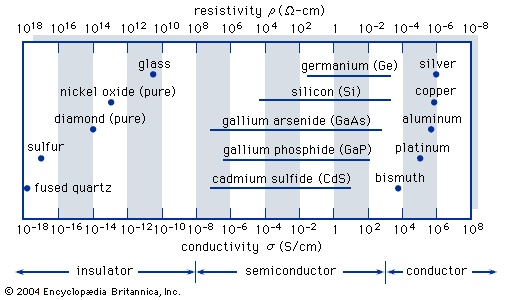 Solid-state materials are commonly grouped into three classes: insulators, semiconductors, and conductors. (At low temperatures some conductors, semiconductors, and insulators may become superconductors (superconductivity).) The figure--> shows the conductivities σ (and the corresponding resistivities ρ = 1/σ) that are associated with some important materials in each of the three classes. Insulators (insulator), such as fused quartz and glass, have very low conductivities, on the order of 10−18 to 10−10 siemens per centimetre; and conductors, such as aluminum, have high conductivities, typically from 104 to 106 siemens per centimetre. The conductivities of semiconductors are between these extremes and are generally sensitive to temperature, illumination, magnetic fields, and minute amounts of impurity atoms. For example, the addition of about 10 atoms of boron (known as a dopant) per million atoms of silicon can increase its electrical conductivity a thousandfold.
 The study of semiconductor materials began in the early 19th century. The elemental semiconductors are those composed of single species of atoms, such as silicon (Si), germanium (Ge), and tin (Sn) in column IV and selenium (Se) and tellurium (Te) in column VI of the periodic table. There are, however, numerous compound semiconductors, which are composed of two or more elements. Gallium arsenide (GaAs), for example, is a binary III-V compound, which is a combination of gallium (Ga) from column III and arsenic (As) from column V. Ternary compounds can be formed by elements from three different columns—for instance, mercury indium telluride (HgIn2Te4), a II-III-VI compound. They also can be formed by elements from two columns, such as aluminum gallium arsenide (AlxGa1 − xAs), which is a ternary III-V compound, where both Al and Ga are from column III and the subscript x is related to the composition of the two elements from 100 percent Al (x=1) to 100 percent Ga (x=0). Pure silicon is the most important material for integrated circuit applications, and III-V binary and ternary compounds are most significant for light emission.
Prior to the invention of the bipolar transistor in 1947, semiconductors were used only as two-terminal devices, such as rectifiers and photodiodes. During the early 1950s germanium was the major semiconductor material. However, it proved unsuitable for many applications, because devices made of the material exhibited high leakage currents at only moderately elevated temperatures. Since the early 1960s silicon has become by far the most widely used semiconductor, virtually supplanting germanium as a material for device fabrication. The main reasons for this are twofold: (1) silicon devices exhibit much lower leakage currents, and (2) silicon dioxide (SiO2), which is a high-quality insulator, is easy to incorporate as part of a silicon-based device. Thus, silicon technology has become very advanced and pervasive, with silicon devices constituting more than 95 percent of all semiconductor products sold worldwide.
Many of the compound semiconductors have some specific electrical and optical properties that are superior to their counterparts in silicon. These semiconductors, especially gallium arsenide, are used mainly for optoelectronic and certain radio frequency (RF) applications.
Electronic properties
 The semiconductor materials described here are single crystals (crystal); i.e., the atoms are arranged in a three-dimensional periodic fashion. Part A of the figure--> shows a simplified two-dimensional representation of an intrinsic (pure) silicon crystal that contains negligible impurities. Each silicon atom in the crystal is surrounded by four of its nearest neighbours. Each atom has four electrons (electron) in its outer orbit and shares these electrons with its four neighbours. Each shared electron pair constitutes a covalent bond. The force of attraction between the electrons and both nuclei holds the two atoms together. For isolated atoms (e.g., in a gas rather than a crystal), the electrons can have only discrete energy levels. However, when a large number of atoms are brought together to form a crystal, the interaction between the atoms causes the discrete energy levels to spread out into energy bands (band theory). When there is no thermal vibration (i.e., at low temperature), the electrons in an insulator or semiconductor crystal will completely fill a number of energy bands, leaving the rest of the energy bands empty. The highest filled band is called the valence band. The next band is the conduction band, which is separated from the valence band by an energy gap (much larger gaps in crystalline insulators than in semiconductors). This energy gap, also called a bandgap, is a region that designates energies that the electrons in the crystal cannot possess. Most of the important semiconductors have bandgaps in the range 0.25 to 2.5 electron volts (electron volt) (eV). The bandgap of silicon, for example, is 1.12 eV, and that of gallium arsenide is 1.42 eV. In contrast, the bandgap of diamond, a good crystalline insulator, is 5.5 eV.
At low temperatures the electrons in a semiconductor are bound in their respective bands in the crystal; consequently, they are not available for electrical conduction. At higher temperatures thermal vibration may break some of the covalent bonds to yield free electrons that can participate in current conduction. Once an electron moves away from a covalent bond, there is an electron vacancy associated with that bond. This vacancy may be filled by a neighbouring electron, which results in a shift of the vacancy location from one crystal site to another. This vacancy may be regarded as a fictitious particle, dubbed a “ hole,” that carries a positive charge and moves in a direction opposite to that of an electron. When an electric field is applied to the semiconductor, both the free electrons (now residing in the conduction band) and the holes (left behind in the valence band) move through the crystal, producing an electric current. The electrical conductivity of a material depends on the number of free electrons and holes (charge carriers) per unit volume and on the rate at which these carriers move under the influence of an electric field. In an intrinsic semiconductor there exists an equal number of free electrons and holes. The electrons and holes, however, have different mobilities; that is, they move with different velocities in an electric field. For example, for intrinsic silicon at room temperature, the electron mobility is 1,500 square centimetres per volt-second (cm2/V·s)—i.e., an electron will move at a velocity of 1,500 centimetres per second under an electric field of one volt per centimetre—while the hole mobility is 500 cm2/V·s. The electron and hole mobilities in a particular semiconductor generally decrease with increasing temperature.
Electrical conduction in intrinsic semiconductors is quite poor at room temperature. To produce higher conduction, one can intentionally introduce impurities (typically to a concentration of one part per million host atoms). This is called doping (dopant), a process that increases conductivity despite some loss of mobility. For example, if a silicon atom is replaced by an atom with five outer electrons, such as arsenic (see part B of the figure-->), four of the electrons form covalent bonds with the four neighbouring silicon atoms. The fifth electron becomes a conduction electron that is donated to the conduction band. The silicon becomes an n-type semiconductor because of the addition of the electron. The arsenic atom is the donor. Similarly, if an atom with three outer electrons, such as boron, is substituted for a silicon atom, an additional electron is accepted to form four covalent bonds around the boron atom, and a positively charged hole is created in the valence band. This creates a p-type semiconductor, with the boron constituting an acceptor.The junction (p-n junction)
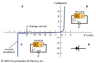 If an abrupt change in impurity type from acceptors (p-type) to donors (n-type) occurs within a single crystal structure, a p-n junction is formed (see parts B and C of the figure-->). On the p side, the holes constitute the dominant carriers and so are called majority carriers. A few thermally generated electrons will also exist in the p side; these are termed minority carriers. On the n side, the electrons are the majority carriers, while the holes are the minority carriers. Near the junction is a region having no free charge carriers. This region, called the depletion layer, behaves as an insulator.
The most important characteristic of p-n junctions is that they rectify. When a forward bias is applied to the p-n junction (i.e., a positive voltage applied to the p-side with respect to the n-side), the majority charge carriers move across the junction so that a large current can flow. However, when a reverse bias is applied, the charge carriers introduced by the impurities move in opposite directions away from the junction, and only a small leakage current flows. As the reverse bias is increased, the leakage current remains very small until a critical voltage is reached, at which point the current suddenly increases. This sudden increase in current is referred to as the junction breakdown, usually a nondestructive phenomenon if the resulting power dissipation is limited to a safe value. The applied forward voltage is typically less than one volt, but the reverse critical voltage, called the breakdown voltage, can vary from less than one volt to many thousands of volts, depending on the impurity concentration of the junction and other device parameters.
Although other junction types have been invented (including p-n-p and n-p-n), p-n junctions remain fundamental to semiconductor devices. For further details on applications on these basic semiconductor properties, see transistor and integrated circuit.
Additional Reading
Simon M. Sze, Physics of Semiconductor Devices, 2nd ed. (1981), is a classic, in-depth treatment of the physics and mathematical models of semiconductor devices. Simon M. Sze (ed.), Modern Semiconductor Device Physics (1998), updates and complements the preceding book.
- Count De la Gardie, Jacob Pontusson
- Count de Maurepas, Jean-Frédéric Phélypeaux
- Count de Montalembert, Charles
- Count De Montemolín Carlos Luis De Borbón
- Count de Rivarol, Antoine Rivaroli
- count d'Erlon Drouet, Jean-Baptiste
- Count de Soissons, Charles de Bourbon
- Count de Soissons, Louis de Bourbon
- Count de Volney, Constantin-François de Chasseboeuf
- Count di Cagliostro, Alessandro
- count d'Orsainville Talon, Jean
- Count d'Unebourg Vandamme, Dominique-René
- Countee Cullen
- countercurrent distribution
- counterespionage
- counterfeiting
- counterintelligence
- counterpoint
- counterpoise
- Counter-Reformation
- countertenor
- countervailing duty
- Countess d' Aulnoy, Marie-Catherine Le Jumel de Barneville
- Countess de Pardo Bazán, Emilia
- Countess di Castiglione, Virginia Oldoini Verasis