semiconductor device
electronics
Introduction
electronic circuit component made from a material that is neither a good conductor nor a good insulator (hence semiconductor). Such devices have found wide applications because of their compactness, reliability, and low cost. As discrete components, they have found use in power devices, optical sensors, and light emitters, including solid-state lasers. They have a wide range of current- and voltage-handling capabilities, with current ratings from a few nanoamperes (10−9 ampere) to more than 5,000 amperes and voltage ratings extending above 100,000 volts. More importantly, semiconductor devices lend themselves to integration into complex but readily manufacturable microelectronic circuits. They are, and will be in the foreseeable future, the key elements for the majority of electronic systems, including communications, consumer, data-processing, and industrial-control equipment.
Semiconductor and junction principles
Semiconductor materials
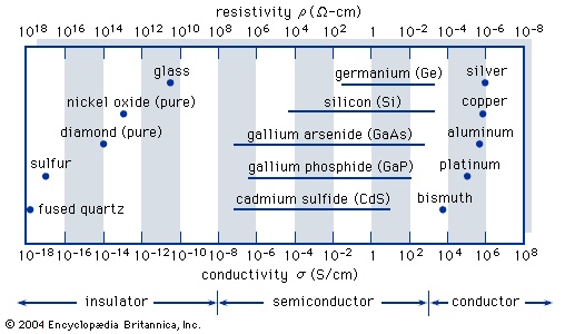 Solid-state materials are commonly grouped into three classes: insulators (insulator), semiconductors, and conductors. (At low temperatures some conductors, semiconductors, and insulators may become superconductors.) Figure 1--> shows the conductivities σ (and the corresponding resistivities ρ = 1/σ) that are associated with some important materials in each of the three classes. Insulators, such as fused quartz and glass, have very low conductivities, on the order of 10−18 to 10−10 siemens per centimetre; and conductors, such as aluminum, have high conductivities, typically from 104 to 106 siemens per centimetre. The conductivities of semiconductors are between these extremes. The conductivity of a semiconductor is generally sensitive to temperature, illumination, magnetic fields, and minute amounts of impurity atoms. For example, the addition of less than 0.01 percent of a particular type of impurity can increase the electrical conductivity of a semiconductor by four or more orders of magnitude (i.e., 10,000 times). The ranges of semiconductor conductivity due to impurity atoms for five common semiconductors are given in Figure 1-->.
 Portion of the periodic table of elements related to semiconductorsThe study of semiconductor materials began in the early 19th century. Over the years, many semiconductors have been investigated. The table (Portion of the periodic table of elements related to semiconductors) shows a portion of the periodic table related to semiconductors. The elemental (chemical element) semiconductors are those composed of single species of atoms, such as silicon (Si), germanium (Ge), and gray tin (Sn) in column IV and selenium (Se) and tellurium (Te) in column VI. There are, however, numerous compound semiconductors that are composed of two or more elements. Gallium arsenide (GaAs), for example, is a binary III-V compound, which is a combination of gallium (Ga) from column III and arsenic (As) from column V.
Ternary compounds can be formed by elements from three different columns, as, for instance, mercury indium telluride (HgIn2Te4), a II-III-VI compound. They also can be formed by elements from two columns, such as aluminum gallium arsenide (AlxGa1 − xAs), which is a ternary III-V compound, where both Al and Ga are from column III and the subscript x is related to the composition of the two elements from 100 percent Al (x = 1) to 100 percent Ga (x = 0). Pure silicon is the most important material for integrated circuit application, and III-V binary and ternary compounds are most significant for light emission.
Prior to the invention of the bipolar transistor in 1947, semiconductors were used only as two-terminal devices, such as rectifiers and photodiodes. During the early 1950s, germanium was the major semiconductor material. However, it proved unsuitable for many applications, because devices made of the material exhibited high leakage currents at only moderately elevated temperatures. Since the early 1960s, silicon has become a practical substitute, virtually supplanting germanium as a material for semiconductor fabrication. The main reasons for this are twofold: (1) silicon devices exhibit much lower leakage currents, and (2) high-quality silicon dioxide (silica) (SiO2), which is an insulator, is easy to produce. Silicon technology is now by far the most advanced among all semiconductor technologies, and silicon-based devices constitute more than 95 percent of all semiconductor hardware sold worldwide.
Many of the compound semiconductors have electrical and optical properties that are absent in silicon. These semiconductors, especially gallium arsenide, are used mainly for high-speed and optoelectronic applications.
Electronic properties
 The semiconductor materials treated here are single crystals (crystal)—i.e., the atoms are arranged in a three-dimensional periodic fashion. Figure 2A--> shows a simplified two-dimensional representation of an intrinsic silicon crystal that is very pure and contains a negligibly small amount of impurities. Each silicon atom in the crystal is surrounded by four of its nearest neighbours. Each atom has four electrons in its outer orbit and shares these electrons with its four neighbours. Each shared electron pair constitutes a covalent bond. The force of attraction for the electrons by both nuclei holds the two atoms together.
At low temperatures the electrons are bound in their respective positions in the crystal; consequently, they are not available for electrical conduction. At higher temperatures thermal vibration may break some of the covalent bonds. The breaking of a bond yields a free electron that can participate in current conduction. Once an electron moves away from a covalent bond, there is an electron deficiency in that bond. This deficiency may be filled by one of the neighbouring electrons, which results in a shift of the deficiency location from one site to another. This deficiency may thus be regarded as a particle similar to an electron. This fictitious particle, dubbed a hole, carries a positive charge and moves, under the influence of an applied electric field, in a direction opposite to that of an electron.
For an isolated atom, the electrons of the atom can have only discrete energy levels (energy state). When a large number of atoms are brought together to form a crystal, the interaction between the atoms causes the discrete energy levels to spread out into energy bands (band theory). When there is no thermal vibration (i.e., at low temperature), the electrons in a semiconductor will completely fill a number of energy bands, leaving the rest of the energy bands empty. The highest filled band is called the valence band. The next higher band is the conduction band, which is separated from the valence band by an energy gap. This energy gap, also called a bandgap, is a region that designates energies that the electrons in the semiconductor cannot possess. Most of the important semiconductors have bandgaps in the range 0.25 to 2.5 eV. The bandgap of silicon, for example, is 1.12 eV and that of gallium arsenide is 1.42 eV.
As discussed above, at finite temperatures thermal vibrations will break some bonds. When a bond is broken, a free electron, along with a free hole, results, i.e., the electron possesses enough thermal energy to cross the bandgap to the conduction band, leaving behind a hole in the valence band. When an electric field is applied to the semiconductor, both the electrons in the conduction band and the holes in the valence band gain kinetic energy and conduct electricity. The electrical conductivity of a material depends on the number of charge carriers (i.e., free electrons and free holes) per unit volume and on the rate at which these carriers move under the influence of an electric field. In an intrinsic semiconductor there exists an equal number of free electrons and free holes. The electrons and holes, however, have different mobilities—that is to say, they move with different velocities in an electric field. For example, for intrinsic silicon at room temperature, the electron mobility is 1,500 square centimetres per volt second (cm2/V·s)—i.e., an electron will move at a velocity of 1,500 centimetres per second under an electric field of one volt per centimetre—while the hole mobility is 500 cm2/V·s. The mobilities of a given semiconductor generally decrease with increasing temperature or with increased impurity concentration.
Electrical conduction in intrinsic semiconductors is quite poor at room temperature. To produce higher conduction, one can intentionally introduce impurities (typically to a concentration of one part per million host atoms). This is the so-called doping process. For example, when a silicon atom is replaced by an atom with five outer electrons such as arsenic (Figure 2C-->), four of the electrons form covalent bonds with the four neighbouring silicon atoms. The fifth electron becomes a conduction electron that is “donated” to the conduction band. The silicon becomes an n-type semiconductor because of the addition of the electron. The arsenic atom is the donor. Similarly, Figure 2C--> shows that, when an atom with three outer electrons such as boron is substituted for a silicon atom, an additional electron is “accepted” to form four covalent bonds around the boron atom, and a positively charged hole is created in the valence band. This is a p-type semiconductor, with the boron constituting an acceptor.The p-n (p-n junction) junction
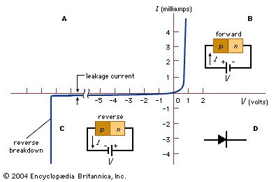 If an abrupt change in impurity type from acceptors (p-type) to donors (n-type) occurs within a single crystal structure, a p-n junction is formed (see Figure 3B--> and 3C-->). On the p side, the holes constitute the dominant carriers and so are called majority carriers. A few thermally generated electrons will also exist in the p side; these are termed minority carriers. On the n side the electrons are the majority carriers, while the holes are the minority carriers. Near the junction is a region having no free-charge carriers. This region, called the depletion layer, behaves as an insulator. The most important characteristic of p-n junctions is that they rectify; that is to say, they allow current to flow easily in only one direction. Figure 3A--> shows the current-voltage characteristics of a typical silicon p-n junction. When a forward bias is applied to the p-n junction (i.e., a positive voltage applied to the p-side with respect to the n-side, as shown in Figure 3B-->), the majority charge carriers move across the junction so that a large current can flow. However, when a reverse bias is applied (in Figure 3C-->), the charge carriers introduced by the impurities move in opposite directions away from the junction, and only a small leakage current flows initially. As the reverse bias is increased, the current remains very small until a critical voltage is reached, at which point the current suddenly increases. This sudden increase in current is referred to as the junction breakdown, usually a nondestructive phenomenon if the resulting power dissipation is limited to a safe value. The applied forward voltage is usually less than one volt, but the reverse critical voltage, called the breakdown voltage, can vary from less than one volt to many thousands of volts, depending on the impurity concentration of the junction and other device parameters.
Two-terminal junction devices
A p-n junction diode is a solid-state device that has two terminals. Depending on impurity distribution, device geometry, and biasing condition, a junction diode can perform various functions. There are more than 50,000 types of diodes with voltage ratings from less than 1 volt to more than 2,000 volts and current ratings from less than 1 milliampere to more than 5,000 amperes. A p-n junction also can generate and detect light and convert optical radiation into electrical energy.
rectifier
This type of p-n junction diode is specifically designed to rectify an alternating current—i.e., to give a low resistance to current flow in one direction and a very high resistance in the other direction. Such diodes are generally designed for use as power-rectifying devices that operate at frequencies from 50 hertz to 50 kilohertz. The majority of rectifiers have power-dissipation capabilities from 0.1 to 10 watts and a reverse breakdown voltage from 50 to more than 5,000 volts. (A high-voltage rectifier is made from two or more p-n junctions connected in series.)
Zener diode
This voltage regulator is a p-n junction diode that has a precisely tailored impurity distribution to provide a well-defined breakdown voltage. It can be designed to have a breakdown voltage over a wide range from 0.1 volt to thousands of volts. The Zener diode is operated in the reverse direction to serve as a constant voltage source, as a reference voltage for a regulated power supply, and as a protective device against voltage and current transients.
Varactor diode
The varactor (variable reactor) is a device whose reactance can be varied in a controlled manner with a bias voltage. It is a p-n junction with a special impurity profile, and its capacitance variation is very sensitive to reverse-biased voltage. Varactors are widely used in parametric amplification, harmonic generation, mixing, detection, and voltage-variable tuning applications.
Tunnel diode
A tunnel diode consists of a single p-n junction in which both the p and n sides are heavily doped with impurities. The depletion layer is very narrow (about 100 angstroms). Under forward biases, the electrons can tunnel or pass directly through the junction, producing a negative resistance effect (i.e., the current decreases with increasing voltage). Because of its short tunneling time across the junction and its inherent low noise (random fluctuations either of current passing through a device or of voltage developed across it), the tunnel diode is used in special low-power microwave applications, such as a local oscillator and a frequency-locking circuit.
Schottky diode
Such a diode is one that has a metal-semiconductor contact (e.g., an aluminum layer in intimate contact with an n-type silicon substrate). It is named for the German physicist Walter H. Schottky, who in 1938 explained the rectifying behaviour of this kind of contact. The Schottky diode is electrically similar to a p-n junction, though the current flow in the diode is due primarily to majority carriers having an inherently fast response. It is used extensively for high-frequency, low-noise mixer and switching circuits. Metal-semiconductor contacts can also be nonrectifying; i.e., the contact has a negligible resistance regardless of the polarity of the applied voltage. Such a contact is called an ohmic contact. All semiconductor devices as well as integrated circuits need ohmic contacts to make connections to other devices in an electronic system.
The p-i-n diode
A p-i-n diode is a p-n junction with an impurity profile tailored so that an intrinsic layer, the “i region,” is sandwiched between a p layer and an n layer. The p-i-n diode has found wide application in microwave circuits. It can be used as a microwave switch with essentially constant depletion-layer capacitance (equal to that of a parallel-plate capacitor having a distance between the plates equal to the i-region thickness) and high power-handling capability.
Bipolar transistors
This type of transistor is one of the most important of the semiconductor devices. It is a bipolar device in that both electrons and holes are involved in the conduction process. The bipolar transistor delivers a change in output current in response to a change in input voltage at the base. The ratio of these two changes has resistance dimensions and is a “transfer” property (input-to-output), hence the name transistor.
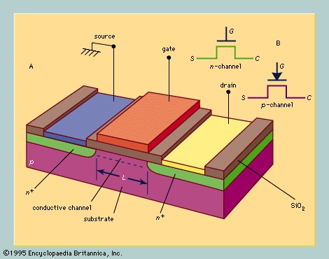
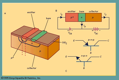 A perspective view of a silicon p-n-p bipolar transistor is shown in Figure 4A-->. Basically the bipolar transistor is fabricated by first forming an n-type region in the p-type substrate; subsequently a p+ region (very heavily doped p-type) is formed in the n region. Ohmic contacts are made to the top p+ and n regions through the windows opened in the oxide layer (an insulator) and to the p region at the bottom. An idealized, one-dimensional structure of the bipolar transistor, shown in Figure 4B-->, can be considered as a section of the device along the dashed lines in Figure 4A-->. The heavily doped p+ region is called the emitter, the narrow central n region is the base, and the p region is the collector. The circuit arrangement in Figure 4B--> is known as a common-base configuration. The arrows indicate the directions of current flow under normal operating conditions—namely, the emitter-base junction is forward-biased and the base-collector junction is reverse-biased. The complementary structure of the p-n-p bipolar transistor is the n-p-n bipolar transistor, which is obtained by interchanging p for n and n for p in Figure 4A-->. The current flow and voltage polarity are all reversed. The circuit symbols for p-n-p and n-p-n transistors are given in Figure 4C-->.
The bipolar transistor is composed of two closely coupled p-n junctions. The emitter-base p+-n junction is forward-biased and has low resistance. The majority carriers (holes) in the p+-emitter are injected (or emitted) into the base region. The base-collector n-p junction is reverse-biased. It has high resistance, and only a small leakage current will flow across the junction. If the base width is sufficiently narrow, however, most of the holes injected from the emitter can flow through the base and reach the collector. This transport mechanism gives rise to the prevailing nomenclature: emitter, which emits or injects carriers, and collector, which collects these carriers injected from a nearby junction.
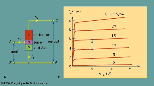 The current gain for the common-base configuration is defined as the change in collector current divided by the change in emitter current when the base-to-collector voltage is constant. Typical common-base current gain in a well-designed bipolar transistor is very close to unity. The most useful amplifier circuit is the common-emitter configuration, as shown in Figure 5A-->, in which a small change in the input current to the base requires little power but can result in much greater current in the output circuit. A typical output current-voltage characteristic for the common-emitter configuration is shown in Figure 5B-->, where the collector current IC is plotted against the emitter-collector voltage VEC for various base currents. A numerical example is provided using Figure 5B-->. If VEC is fixed at five volts and the base current IB is varied from 10 to 15 microamperes (μA; 1 μA = 10−6 A), the collector current IC will change from about four to six milliamperes (mA; 1 mA = 10−3 A), as can be read from the left axis. Therefore, an increment of 5 μA in the input-base current gives rise to an increment of 2 mA in the output circuit—an increase of 400 times, with the input signal thus being substantially amplified. In addition to their use as amplifiers, bipolar transistors are key components for oscillators and pulse and analog circuits, as well as for high-speed integrated circuits. There are more than 45,000 types of bipolar transistors for low-frequency operation, with power outputs up to 3,000 watts and a current rating of more than 1,000 amperes. At microwave frequencies, bipolar transistors have power outputs of more than 200 watts at 1 gigahertz and about 10 watts at 10 gigahertz.
 Thyristors (thyristor)
The thyristors constitute a family of semiconductor devices that exhibit bistable characteristics and can be switched between a high-resistance, low-current “off” state and a low-resistance, high-current “on” state. The operation of thyristors is intimately related to the bipolar transistor, in which both electrons and holes are involved in the conduction processes. The name thyristor is derived from the electron tube called the gas thyratron, since the electrical characteristics of both devices are similar in many respects. Because of their two stable states (on and off) and low power dissipations in these states, thyristors are used in applications ranging from speed control in home appliances to switching and power conversion in high-voltage transmission lines. More than 40,000 types of thyristors are available, with current ratings from a few milliamperes to more than 5,000 amperes and voltage ratings extending to 900,000 volts.
 Figure 6A--> provides a perspective view of a thyristor structure. An n-type wafer is generally chosen as the starting material. Then, a diffusion step is used to form the p1 and p2 layers simultaneously by diffusing the wafer from both sides. (Diffusion is the movement of impurity atoms into the crystalline structure of a semiconductor.) Finally, n-type impurity atoms are diffused through a ring-shaped window in an oxide into the p2 region to form the n2 layer.A cross section of the thyristor along the dashed lines is shown in Figure 6B-->. The thyristor is a four-layer p-n-p-n diode with three p-n junctions in series. The contact electrode to the outer p layer (p1) is called the anode, and that to the outer n layer (n2) is designated the cathode. An additional electrode, known as the gate electrode, is connected to the inner p layer (p2).The basic current-voltage characteristic of a thyristor is illustrated in Figure 6C-->. It exhibits three distinct regions: the forward-blocking (or off) state, the forward-conducting (or on) state, and the reverse-blocking state, which is similar to that of a reverse-biased p-n junction. Thus, a thyristor operated in the forward region is a bistable device that can switch from a high-resistance, low-current off state to a low-resistance, high-current on state, or vice versa.In the forward off state, most of the voltage drops across the centre n1-p2 junction, while in the forward on state all three junctions are forward-biased. The forward current-voltage characteristic can be explained using the method of a two-transistor analog—that is, to consider the device as a p-n-p transistor and an n-p-n transistor connected with the base of one transistor (n1) attached to the collector of the other. As the voltage VAK in Figure 6C--> increases from zero, the current IA will increase. This in turn causes the current gains of both transistors to increase. Because of the regenerative nature of these processes, switching eventually occurs, and the device is in its on state. The maximum forward voltage that can be applied to the device prior to switching is called the forward-breakover voltage VBF. The magnitude of VBF depends on the gate current. Higher gate currents cause the current IA to increase faster, enhance the regeneration process, and switch at lower breakover voltages. The effect of gate current on the switching behaviour is shown in Figure 6C--> (dotted line).
A bidirectional, three-terminal thyristor is called a triac. This device can switch the current in either direction by applying a small current of either polarity between the gate and one of the two main terminals. The triac is fabricated by integrating two thyristors in an inverse parallel connection. It is used in AC applications such as light dimming, motor-speed control, and temperature control. There also are many light-activated thyristors that use an optical signal to control the switching behaviour of devices.
Metal-semiconductor field-effect transistors
The metal-semiconductor field-effect transistor (MESFET) is a unipolar device, because its conduction process involves predominantly only one kind of carrier. The MESFET offers many attractive features for applications in both analog and digital circuits. It is particularly useful for microwave amplifications and high-speed integrated circuits, since it can be made from semiconductors with high electron mobilities (e.g., gallium arsenide, whose mobility is five times that of silicon). Because the MESFET is a unipolar device, it does not suffer from minority-carrier effects and so has higher switching speeds and higher operating frequencies than do bipolar transistors.
 A perspective view of a MESFET is given in Figure 7A-->. It consists of a conductive channel with two ohmic contacts, one acting as the source and the other as the drain. The conductive channel is formed in a thin n-type layer supported by a high-resistivity semi-insulating (nonconducting) substrate. When a positive voltage is applied to the drain with respect to the source, electrons flow from the source to the drain. Hence, the source serves as the origin of the carriers, and the drain serves as the sink. The third electrode, the gate, forms a rectifying metal-semiconductor contact with the channel. The shaded area underneath the gate electrode is the depletion region of the metal-semiconductor contact. An increase or decrease of the gate voltage with respect to the source causes the depletion region to expand or shrink; this in turn changes the cross-sectional area available for current flow from source to drain. The MESFET thus can be considered a voltage-controlled resistor.A typical current-voltage characteristic of a MESFET is shown in Figure 7B-->, where the drain current ID is plotted against the drain voltage VD for various gate voltages. For a given gate voltage (e.g., VG = 0), the drain current initially increases linearly with drain voltage, indicating that the conductive channel acts as a constant resistor. As the drain voltage increases, however, the cross-sectional area of the conductive channel is reduced, causing an increase in the channel resistance. As a result, the current increases at a slower rate and eventually saturates. At a given drain voltage the current can be varied by varying the gate voltage. For example, for VD = 5 V, one can increase the current from 0.6 to 0.9 mA by forward-biasing the gate to 0.5 V, as shown in Figure 7B-->, or one can reduce the current from 0.6 to 0.2 mA by reverse-biasing the gate to −1.0 V.
A device related to the MESFET is the junction field-effect transistor (JFET). The JFET, however, has a p-n junction instead of a metal-semiconductor contact for the gate electrode. The operation of a JFET is identical to that of a MESFET.
There are basically four different types of MESFET (or JFET), depending on the type of conductive channel. If, at zero gate bias, a conductive n channel exists and a negative voltage has to be applied to the gate to reduce the channel conductance, as shown in Figure 7B-->, then the device is an n-channel “normally on” MESFET. If the channel conductance is very low at zero gate bias and a positive voltage must be applied to the gate to form an n channel, then the device is an n-channel “normally off” MESFET. Similarly, p-channel normally on and p-channel normally off MESFETs are available.To improve the performance of the MESFET, various heterojunction field-effect transistors (FETs) have been developed. A heterojunction is a junction formed between two dissimilar semiconductors, such as the binary compound GaAs and the ternary compound AlxGa1 − xAs. Such junctions have many unique features that are not readily available in the conventional p-n junctions discussed previously.
 Figure 8--> shows a cross section of a heterojunction FET. The heterojunction is formed between a high-bandgap semiconductor (e.g., Al0.4Ga0.6As, with a bandgap of 1.9 eV) and one of a lower bandgap (e.g., GaAs, with a bandgap of 1.42 eV). By proper control of the bandgaps and the impurity concentrations of these two materials, a conductive channel can be formed at the interface of the two semiconductors. Because of the high conductivity in the conductive channel, a large current can flow through it from source to drain. When a gate voltage is applied, the conductivity of the channel will be changed by the gate bias, which results in a change of drain current. The current-voltage characteristics are similar to those of the MESFET shown in Figure 7B-->. If the lower-bandgap semiconductor is a high-purity material, the mobility in the conductive channel will be high. This in turn can give rise to higher operating speed.
Metal-oxide-semiconductor field-effect transistors
The most important device for very-large-scale integrated circuits (those that contain more than 100,000 semiconductor devices such as diodes and transistors) is the metal-oxide-semiconductor field-effect transistor (MOSFET). The MOSFET is a member of the family of field-effect transistors, which includes the MESFET and JFET.
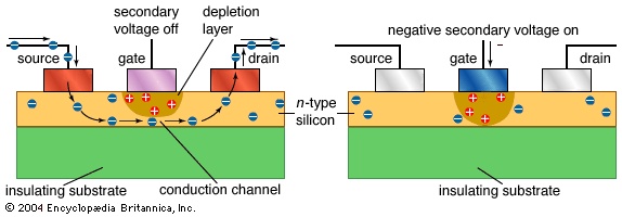
 A perspective view for an n-channel MOSFET is shown in Figure 9-->. Although it looks similar to a MESFET, there are four major differences: (1) the source and drain of a MOSFET are rectifying p-n junctions instead of ohmic contacts; (2) the gate is a metal-oxide-semiconductor structure, meaning that there is an insulator—silicon dioxide (SiO2)—sandwiched between the metal electrode and the semiconductor substrate, while for the MESFET the gate electrode forms a metal-semiconductor contact; (3) the left edge of the gate electrode must be aligned or overlapped with the source contact to facilitate device operation, while in a MESFET there is no overlapping of gate and source contact; and (4) the MOSFET is a four-terminal device, so that there is a fourth substrate contact in addition to the source, drain, and gate electrode, as in the case of a MESFET.One of the key device parameters is the channel length, L, which is the distance between the two n+-p junctions, as indicated in Figure 9-->. When the MOSFET was first developed, in 1960, the channel length was longer than 20 micrometres (μm). Today channel lengths less than 1 μm have been fabricated in volume production, and lengths less than 0.1 μm have been created in research laboratories.
The source is generally used as the voltage reference and is grounded. When no voltage is applied to the gate, the source-to-drain electrodes correspond to two p-n junctions connected back to back. The only current that can flow from source to drain is a small leakage current. When a high positive bias is applied to the gate, a large number of electrons will be attracted to the semiconductor surface and form a conductive layer just underneath the oxide. The n+ source and n+ drain are now connected by a conducting surface n layer (or channel) through which a large current can flow. The conductance of this channel can be modulated by varying the gate voltages; the conductance also can be changed by the substrate bias.
The current-voltage characteristic of a MOSFET is similar to that shown in Figure 7B-->. There are also four different kinds of MOSFETs, depending on the type of conducting layer. The four are n-channel normally off, n-channel normally on, p-channel normally off, and p-channel normally on MOSFETs. They are similar to MESFET varieties.The main reasons why the MOSFET has surpassed the bipolar transistor and become the dominant device for very-large-scale integrated circuits are: (1) the MOSFET can be easily scaled down to smaller dimensions, (2) it consumes much less power, and (3) it has relatively simple processing steps, and this results in a high manufacturing yield (i.e., the ratio of good devices to the total).
- Santa Elena Peninsula
- Santa Fe
- Santa Fe Island
- Santa Fe Trail
- Santa Gertrudis
- Santa Hermandad
- Santa Isabel
- Santalaceae
- Santalales
- Santali language
- Santa Lucia Range
- Santa Luzia Island
- Santa Maria
- Santa Maria dei Frari
- Santa Maria Island
- Santa Maria Novella
- Santa Marta
- Santa Marta Mountains
- Santa María
- Santa María Island
- Sant'Ambrogio Basilica
- Santa Monica
- Santana
- Santander
- Santander, Francisco de Paula